
13.56 MHz WPT for Medical Devices: From simulation to coil design

July 28, 2026
Wireless power transfer (WPT) is becoming the standard way to recharge implantable medical devices. In active implantable medical devices (AIMDs) like neurostimulators, power demands are high enough that batteries alone can't keep up. Recharging has to happen wirelessly, and 13.56 MHz in the ISM band has become one of the most widely adopted frequencies for this.
But implanted coils don't play by ideal-world rules. Misalignment is the norm, not the exception, and the link has to work through a lossy medium: biological tissue. This not only changes the link's properties, but also brings its own hard limit. Specific Absorption Rate (SAR) caps how much energy the tissue can safely absorb.
On top of that, the system still has to guarantee a target power delivered to the load (PDL), so the device recharges predictably regardless of the coupling conditions it lands in. The usual fix, simply pushing more transmitted power, runs directly into a wall of constraints: EMI regulations, SAR limits, and heating on both the Tx and Rx sides.
Designing a coil and power transfer circuit for this kind of link means balancing all of these limits at once. There's no single closed-form answer to lean on. What follows is the methodology we've been using here at Focus to work through that trade-off space: starting with link modeling, running electromagnetic simulations against it, and iterating from there toward a coil design that holds up in practice.
The basics for designing a WPT Link
The image below shows the basic components for a WPT link many may be familiar with. The main components, the Tx and Rx coils, are inductively coupled with a coupling factor k, which depends on the coils' geometry, construction, and alignment. Power transmission is driven in the Tx by a voltage source driving the circuit at the WPT frequency, f₀.

Using the reflected load theory, the links WPT power transfer efficiency (PTE) and the power delivered to the load (PDL) can be calculated as follows under resonant Tx and Rx hypothesis:

Where Q_Tx is the quality factor of the transmission coil, Q_Rx is the quality factor of the reception coil, and k is the coupling factor of the link. As can be seen, the PDL and PTE are governed by the quality factors and the coupling coefficient. For a given PTE, achieving the desired PDL only requires increasing the voltage source amplitude. Furthermore, given the coupling factor and the coils' Q, there are optimal RL values that maximize either PDL or PTE.
RL is the equivalent load seen by the Rx matching network. This load is determined by the Rx circuit, which usually consists of a rectifier plus some kind of regulator.
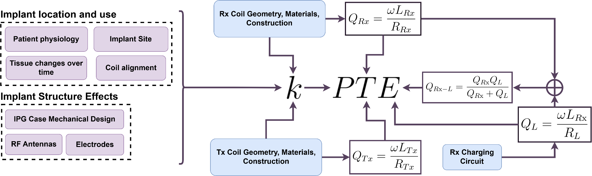
The following diagram summarizes how all the links parameter are affected by de different design constraints:
Design methodology
To design a WPT link for a medical device, we built a top-down methodology at Focus. It starts from the theoretical foundations of the link and progressively adds non-idealities, so the final design is robust enough to meet the demands of this application. The image below shows the full process.

Requirements
The first step is to pin down the link requirements. This comes directly from the medical device design process and is key to setting realistic specifications without over-engineering.
We focus on two: battery size and target charging time. Battery size follows from the IPG's overall target size and the desired battery life; charging time follows from the user experience we want to deliver and what is technologically feasible. From these two, we derive the Power Delivered to the Load (PDL) needed to complete a charge cycle in the target time, plus enough headroom.
That headroom accounts for the inefficiencies of the Rx circuit and for how link efficiency changes during normal use. Estimating it means working through the expected coil misalignment and any variation in the vertical distance between the transmit and receive coils.
We also study the regulatory requirements early. The two main constraints are the Specific Absorption Rate (SAR) and the electromagnetic interference (EMI) the device generates. Both cap the transmission power available to us, and we revisit them at a later step, so from the start we identify the limits set by the relevant regulatory bodies. For example, the FCC limits (47 CFR §15.209, §15.205, and Part 18 for ISM) set the electric field strength at 3 meters to no more than 30 µV/m in the ISM band, and cap SAR for the general population at 1.6 W/kg, averaged over any 1g of tissue.
Setting requirements is itself iterative. Requirements will likely shift as development progresses, but we need a reference point to design from.
Design space exploration
Next, we explore the design space through the link's key parameters at a given WPT frequency: the coupling factor and the coil quality factors. This usually takes the form of efficiency level curves across k and the quality factors. Combined with the PDL requirement, these curves let us define a target design space for the coil quality factors that keeps efficiency high enough.
The logic is direct: the higher the PDL needed at the Rx side, the higher the transmitted power required, and therefore, for a given efficiency, the higher the emissions and SAR.

Rx WPT circuit
We design the Rx power management and battery management circuits, usually requiring a rectifier, a voltage regulator, and finally a battery charger. This design is highly constrained by both available area and safety considerations. We have to account for heating while minimizing circuit area.
The charging load and the inefficiencies of the regulators and rectifier determine the final impedance seen by the matching network (MN). We design the MN to both optimize the PDL and achieve resonance at the desired frequency with the Rx coil.
Driver design
This stage turns the DC supply and the switching waveform into RF power for the coil. We build it as a Class-E amplifier, which reaches near-total efficiency under zero-voltage switching but ties its performance to the load: as coupling shifts with distance and alignment, the amplifier detunes, switching losses climb, and the device sees higher voltage stress.
A Class-D topology trades some of that peak efficiency for better tolerance to load variation and lower device stress, at the cost of a second switch and harder high-side gate drive at 13.56 MHz. The drive scheme itself also shapes the emissions, so we explore soft-switching, controlled gate slew, harmonic-aware driving techniques, and output filtering to hold EMI down.
Coil design, Tx and Rx
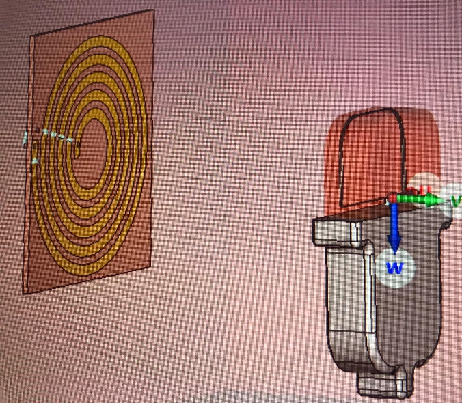
We select the technology, materials, and mechanical constraints for each coil. The Rx coil is the most constrained, since implant geometry leaves little room to work with. Additionally, if the coil must be implemented as part of the header, it must be constructed from biocompatible materials such as platinum-iridium, which has lower conductivity than copper. We design both coils through EM simulation in tools such as CST, exploring Q and k across the coil pair. From those simulations, we extract the series resistance at the operating frequency, along with Q and inductance, and these values drive the MN design.
One point deserves emphasis: build the coils. EM simulation is powerful, but simulating series resistance with high precision at high frequency is genuinely hard. We recommend building coil prototypes, measuring them directly with the right tools, and driving the design from those measurements. We can't design matching networks from simulated values alone; they need real coils to tune against.
Full circuit simulation
With a first design for every component in place, we run a full circuit simulation, usually in SPICE-based tools, where every part of the circuit comes together. The goal is to confirm whether the target PDL is achievable.

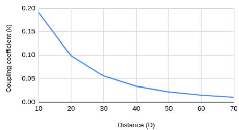
Once the idealized link hits its target, we add back the complexity we set aside, checking PDL after each step. We start with the effect of human tissue and the device's mechanical design on the link, using EM simulation to evaluate how tissue between the coils changes the coupling factor. The device's metallic body, any RF antennas in the magnetic flux path, and the leads all affect k as well. We then vary implant depth and coil misalignment across realistic estimates to find the minimum expected k, and from that we derive the maximum Tx power needed to reach the target PDL.
At that maximum power, we simulate SAR and confirm it stays within the regulatory limit, such as the FCC's SAR threshold. For EMI, we account for the fields from both the coil and the driving circuit. We can simulate coil EMI in EM software and measure it per the FCC standard. The driving circuit is harder, since fitting the full circuit into an EM field solver is impractical. Our approach is to import the PCB layout into the EM tool, many of which support this, and combine it with the SPICE-simulated currents and voltages. Some tools also allow mixed SPICE-EM simulation, where we bring the whole driving circuit in directly. Finally, we check component heating on both Tx and Rx against the limits in the relevant standards, with particular attention to the driving circuit, which must run at high efficiency to avoid unnecessary heat.
Each pass through this loop tightens the design against every constraint we started with, not just the idealized case, before we move on to prototyping and testing.
Conclusions
There is no single closed-form answer to a WPT link for an implant, and that is the point. The coupling shifts, the tissue takes its cut, and SAR, EMI, and heating each pulls against the transmitted power we would otherwise reach for.
The methodology we've built at Focus treats that as the starting condition rather than a problem to wish away: fix the requirements, map the design space through k and the coil quality factors, and then layer the real-world non-idealities back in one at a time, checking PDL against every constraint as we go. What comes out the other side is not a theoretically perfect link. It is one that holds its target power across the misalignment, depth, and load variation an implant actually sees, and is capable of passing the design verification stage.
That is the trade-off space this whole process exists to navigate, and working it iteratively, from link model to EM simulation to measured prototypes, is what gets a design from a level curve on a plot to hardware that recharges a device predictably inside the body.
Get in touch
If you're working through a WPT link for an implantable device and want a second set of eyes on where it's landing on this trade-off space, we're glad to talk through it. Reach out to the Focus Medical Studio team.
Stay focused on what’s next
Stories, ideas, and insights from the world of technology, product development, and innovation.




© Copyright 2026 Focus. All Rights Reserved.