
Faster PCB Production: What Manufacturers Actually Need

August 27, 2026
Wrapping up a layout must be one of the most exciting (and scary) moments a hardware engineer faces. My components are all perfectly placed and routed; the circuits I designed and simulated satisfy all the product requirements. I even took every recommended precaution for DFM and DFA in my layout. There is no way this can go wrong.
And then, just like a kid who writes a letter to Santa asking for a red bike, we send our Gerber files off; only to receive, in response, tons of "could you please confirm…", "could you please clarify…". Suddenly, an easy-to-manufacture PCB that was going to take two weeks ends up taking a month, just because we, the engineers, are the only geniuses who understand the board, and everyone else is the problem.
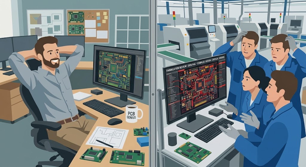
But the real problem is that fabricating and assembling a PCB is not a simple task at all. Correct DFM and DFA isn't only about ensuring correct clearances; it's about understanding every difficulty of the multidisciplinary manufacturing process, so there's no doubt about what's expected from the manufacturer. That way, manufacturing can move quickly, and we don't end up receiving a blue skateboard instead of our beautiful red bike.
A PCB is not a printout
Manufacturing a PCB must be one of the most complex, labor-intensive processes out there; it combines chemistry, mechanics, and electronics into a single sequence where every step has its own tolerances. It's not as simple as a printer outputting our Gerber files, as if they were copper A4 sheets, later pressed and drilled.
Between the design file and the finished board there's a long chain of processes, and each one has its own way of turning a clean design into a headache. Traces that looked perfectly fine in the layout tool can end up close enough to bridge once etching tolerances come into play. A via can land slightly off target when layer-to-layer registration drifts, especially on boards where annular rings are already pushed to their limit.
We've seen components rotate mid-reflow simply because solder paste wasn't properly balanced across their pads, pulling the part off center as the paste melted unevenly on each side. Plating doesn't always build up evenly inside a deep via on a multilayer stack either, and on panelized boards, a breakout tab placed too close to a component can crack the board right at the edge during depaneling.
None of these failures happen because the data was wrong. They happen because tolerances compound across a dozen processes at once, and the manufacturer is the one who has to catch, absorb, or push back on that variability before it becomes a defective batch. That's why yield isn't just a function of good files; it's a function of how much certainty the manufacturer has about what the design actually requires, and how much room they have to make judgment calls where the documentation stays silent.
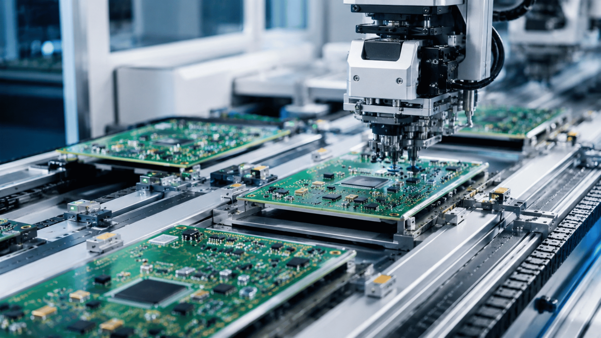
Long and tedious DFM checks from the manufacturer are usually the result of that missing certainty; a gap in what's communicated, or when it's communicated. The hardware engineer should always anticipate the questions a manufacturer will have, so the process moves quickly and without friction, without putting quality or timeline at risk.
What does a manufacturer really need?
Gerbers, NC drill files, and pick-and-place files, together with the BOM right? Well, That's technically true; with this set of files, a manufacturer already has what's needed to start building a PCB. Gerbers and NC drill files are what the fabricator needs to build the bare board, while pick-and-place and the BOM are what the Contract Manufacturer (CM) needs to assemble it.
For simple boards, or for early proof-of-concept stages, quantities are typically low and the required capabilities or specs are minimal. In that context, we can usually tolerate a lower yield, since a higher failure percentage on a handful of boards is a manageable cost, not a production risk. But when timelines are critical, or the board carries specific mechanical or electrical requirements, understanding the manufacturing process and anticipating the questions the manufacturer will have, becomes key.
This is why a proper manufacturer release package is never just the raw input files an EMS feeds into its machines. If we want reliability and a friction-free process with a fabricator, the package also needs to correctly document the board itself. That documentation is what removes the guesswork, and it's precisely what turns a two-week build into a two-week build, instead of a month of back-and-forth.
The Focus Way:
At Focus, we see ourselves not just as an engineering shop, but as an engineering partner. That means understanding the processes and pitfalls that show up along the way from an idea to a finished product, not just the engineering itself. In that context, anticipating problems before they surface is essential.
Across hundreds of projects and PCB designs, guessing which questions a manufacturer is about to ask is something we have learnt to do. We make sure the release package answers them before they're asked. It's less about getting everything right on the first try, and more about knowing where boards typically run into friction, so that friction never gets the chance to show up.
Know your manufacturer
"I will always communicate with my manufacturer as soon as I start my layout, not at the end." That's what I'd make every HW engineer write a hundred times on a whiteboard during onboarding, if HR would let me.
Our PCBs have to adapt to real manufacturing capabilities; we can't expect a manufacturer's capabilities to adapt to our requirements. The road to failure, and to a painfully low yield, is designing at the edge of generic manufacturing capabilities, or building a stack-up we assumed rather than confirmed, only to find out later that real-world tolerances are far looser than what we can actually work with, or that the board can't be built as designed at all.
This is exactly why talking to the manufacturer early matter, it's how design rules get built on a real stack-up and real capabilities from the beginning, instead of being adjusted after
Where AI Actually Helps
We know that in hardware development, the use of AI isn't yet as obvious or as mature as it is in other kinds of workflows. Some tools are still too expensive to justify given their current results, and integrating LLMs with KiCad is possible but not exactly simple or automatic, let alone in tools like Altium, where it isn't even possible yet.
But that doesn't mean AI can't be integrated into the workflow to automate tasks that used to be slow or tedious, like automatically checking stock availability for our BOMs, or correctly matching part numbers against component descriptions in BOMs with hundreds of lines.
Generating scripts to automatically compare our boards against a manufacturer's capabilities, or other one-off scripts tailored to a specific PCB, are other examples of tools we've built into our workflow at Focus, ones that end up saving hours during the handoff to manufacturing, and countless rounds of back-and-forth.
Make use of mechanical layers
Tell your manufacturer about every detail you consider important on the mechanical layers: designators, component orientation, clearances, mechanical mounting points, keep-out zones, tooling hole or fiducial locations, etc.
Clarifying things that seem obvious to us can save a lot of back-and-forth with manufacturers. Mechanical layers let us flag specific characteristics of a given area on the PCB that we want to make sure don't get missed.
Always provide drawings
Most people completely overlook what a Draftman document in Altium (or an equivalent fab/assembly drawing) can actually do. It's more commonly associated with the jump to production than with prototypes, but having it well built becomes critical the moment a PCB carries demanding specs or complex technology features, like high-power boards or HDI stack-ups.
This is where you specify the IPC class your board needs to meet, so the manufacturer knows exactly which tolerances apply. It's also where microvia and plugged/filled via requirements get called out, where the stack-up and dielectric materials needed to hit target impedance on high-speed nets are defined, and where controlled impedance traces get tied back to a real transmission line structure table instead of being left to guesswork. None of this lives in the Gerbers; it lives in the drawing.
Without a well-detailed drawing, a lot of that critical information ends up camouflaged inside the Gerbers or NC Drill files instead, buried in a layer name or a hole table with no context around it. Some of it makes it through, some of it doesn't, and the manufacturer is left guessing at requirements that were never really communicated in full.
The Draftsman documents should be the identity of our PCB, the single reference a manufacturer can point to for every requirement the board needs to meet, from drilling tolerances and plating specs to testing requirements like electrical test or microsection, and, on the assembly side, traceability, inspection class, and keep-out areas for conformal coating. When that drawing is missing or incomplete, all of that ends up being negotiated over email, one board revision at a time.
Conclusion
After reading this article, I hope the lesson you take away is "I WILL ALWAYS COMMUNICATE WITH MY MANUFACTURER AS SOON AS I START MY LAYOUT, NOT AT THE END." Sending your PCB to be manufactured isn't just about providing the files for the machine that will print and assemble your board, it's a communication task involving large, multidisciplinary teams.
A successful manufacturing process only begins once the EMS understands exactly what it needs to build, and what success actually looks like for that specific PCB. Nobody knows that better than us, the engineers, so making it clear is our job. At Focus, after hundreds of PCBs sent to manufacturing, this is a conversation we know how to have, so don't hesitate to reach out if you need help taking this next step.
.webp)
Stay focused on what’s next
Stories, ideas, and insights from the world of technology, product development, and innovation.



© Copyright 2026 Focus. All Rights Reserved.